8×8 Register Bank with Clock Gating
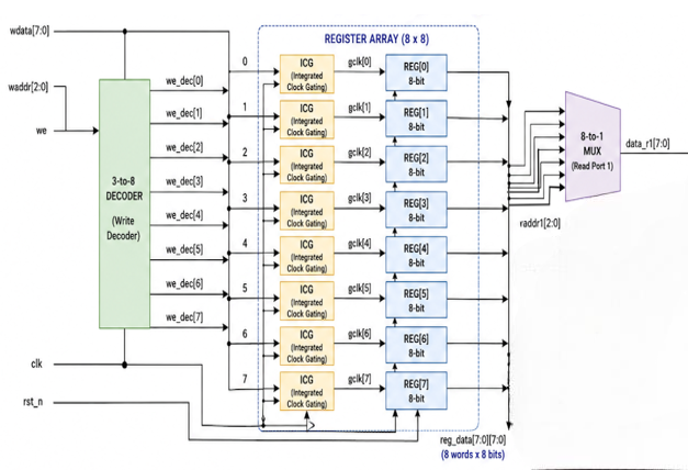
A documented team project for an 8-register × 8-bit bank with one write port, one read port, and a latch-based Integrated Clock Gating path.
My role
Team member; the report does not isolate individual subsystem ownership.
Project visuals
Measured results
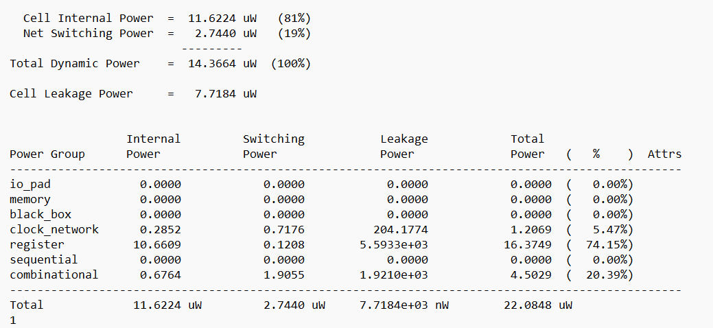
Dynamic power estimate49.61 → 14.37 μWNoGate → gated; −71.0%
Total power estimate59.75 → 22.08 μWNoGate → gated; −63.0%
Cell area estimate559.66 → 462.31NoGate → gated; −17.4%
Reported timing slackSetup +3.65 ns / Hold +0.81 nsGated design
Design objectives
- Build an 8 × 8-bit register array with a 3-to-8 write decoder and read multiplexer.
- Verify the clock-gated and no-gate variants with constrained-random transactions and a scoreboard.
- Compare synthesis estimates, timing slack, switching activity, and a physical implementation flow.
Implementation approach
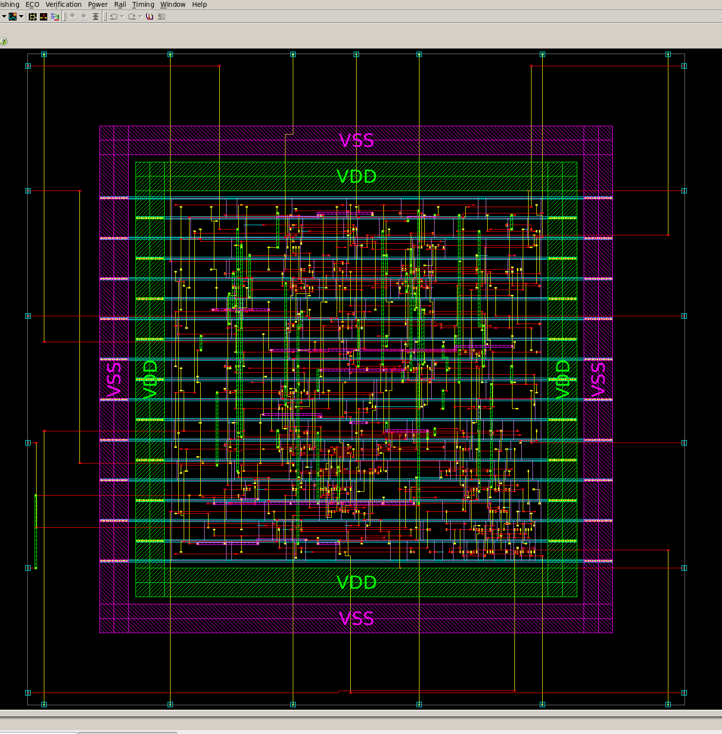
The report describes a manually implemented latch-based clock_gate_latch with a test_en bypass, per-register gating, Design Compiler synthesis, and an IC Compiler flow covering floorplan, power planning, placement, CTS, and routing.
Scope and limitations
Area and power are reported synthesis estimates for NoGate versus clock-gated variants, not silicon measurements. The IC Compiler connectivity check reports unused QN pins; the report does not establish clean DRC/LVS sign-off.