2.4 GHz PLL with Dual-Modulus Divider
A TSMC 180 nm schematic-level PLL project targeting 2.4 GHz, a 1 MHz step, and a total divide ratio N=2400.
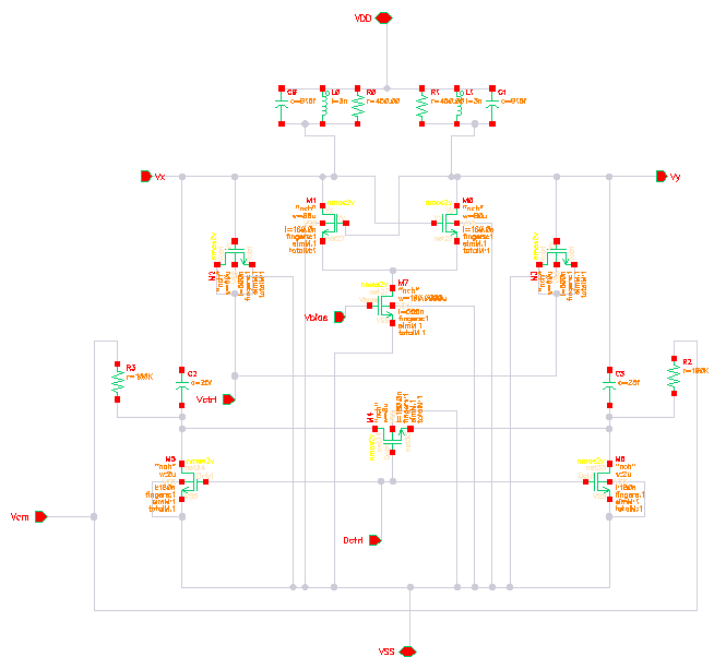
My role
Assigned team contribution: LC-VCO and frequency divider, as listed in the report's contribution table.
Project visuals
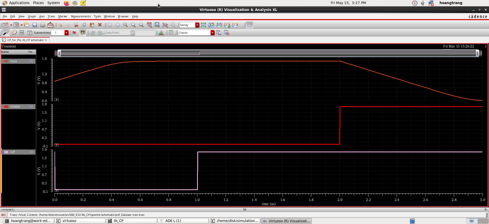
Measured results
VCO center2.400 GHzTSMC 180 nm; schematic-level
Fine tuning2.346–2.479 GHzVctrl 0.3–1.5 V
Phase noise−114.33 dBc/Hz1 MHz offset
DividerN=2400 → 1 MHzDIV8 + DIV300
VCO power≈5.9 mWPre-layout simulation
Design objectives
- Design and simulate a differential NMOS cross-coupled LC-VCO around 2.4 GHz.
- Build a DIV8 + DIV300 path for N=2400 and a 1 MHz feedback signal.
- Connect the blocks conceptually across PFD, charge pump, loop filter, VCO, and divider.
Implementation approach
The report uses TSMC 180 nm and 1.8 V schematic-level simulations. The VCO is checked with PSS/PNoise, fine/coarse tuning, and phase-noise measurements; the divider uses DIV8, a 9-bit counter, detect/reset logic, and DIV300.
Scope and limitations
Results are pre-layout/schematic-level. The report does not provide a verified final lock time or post-layout parasitic/EM extraction.